
Guangdong Inmark Electronics Co., Ltd. was founded in 2011. It is a well-known domestic high-tech semiconductor packaging and testing enterprise and a national-level "little giant" enterprise dedicated to providing high-quality semiconductor components and products to global electronic manufacturing companies. To date, Inmark Electronics has two major production bases: Shenzhen Factory in the Pearl River Delta and Yancheng, Jiangsu in the Yangtze River Delta, with a construction area of 40,000 square meters. The current packaging and testing workshop area is 20,000 square meters. The main packaging forms are SOT, TO series, and PDFN product packaging. With the company's investment and continuous optimization of process technology, the quality has been steadily improved. It has established strategic partnerships with well-known companies in the industry and has developed into a highly competitive power device packaging and testing company in the country.
Inmark Electronics currently has a total of more than 500 employees, including more than 100 R&D personnel. Since its establishment, the company has focused on the research and development, design, production and sales of semiconductor chips and power devices such as MOSFET and IGBT. The products are of high quality and complete series, covering the system applications of mainstream integrated circuits. Main products: Schottky diodes, triodes, low/middle/high voltage MOS, fast recovery diodes, low vf Schottky, IGBT, etc., widely used in consumer electronics, automotive electronics, industrial electronics, new energy vehicles and charging piles, intelligent equipment manufacturing, rail transportation, photovoltaic new energy, 5G and other fields.
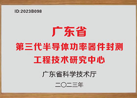
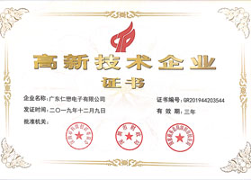
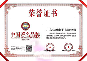
Inmark Electronics insists on independent research and development and manufacturing, breaking foreign technical barriers, and promoting the localization of silicon carbide automotive chips. At present, the company has applied for/obtained nearly 100 patents to form a three-dimensional intellectual property protection system, and established its own brand MOT. At the same time, it has introduced world-class high-end equipment with a high degree of automation to ensure the stability of the product. The semiconductor device packaging and testing production line is at the world's advanced level, providing a solid foundation for modern large-scale production.
Inmark Electronics gathers talents, with academicians, ph.D. holder and other industry leaders as the core. And relying on its comprehensive advantages in technology, brand, channels, etc. to develop international advanced power device packaging and manufacturing technology, fully promote the research and development and industrialization of high-end power MOSFET, IGBT, and integrated power devices, and continue to deploy advanced and cutting-edge technology fields of semiconductor power devices, enhance the competitiveness and market position of the company's core products, deepen the comprehensive localization of products, innovate, provide high-quality products, and develop energy-saving and sustainable solutions for our customers. Inmark Electronics has established an efficient supply chain management process, and its annual shipments can exceed 10 billion units, meeting the stringent requirements of the market and customers.


 Address:19th Floor, SCTC Mansion, Guiyuan Rd, Luohu, Shenzhen
 Tel:+86-755-82527851