


Today, we'll take a look at one classic component that is likely to be used extensively.
Taking Inmark’s MOT80N03D as an example,we will know how a seemingly ordinary MOSFET becomes the cornerstone of reliable BMS operation, and its in-depth considerations in BOM selection.
Device Focus: Inmark’s MOT80N03D, a balanced "Guardian"
In the discharging protection circuit of a BMS, we often see multiple MOSFETs connected in parallel to share the large current. The Inmark’s MOT80N03D is a 30V and 80A N-channel MOSFET, the core advantage lies in its excellent cost-effectiveness and reliable robustness.
Key Parameters at a glance:
*Vds = 30V: Perfectly covers mainstream 3.7V lithium-ion cell in 7-cell configurations (approximately 29.4V when fully charged), with ample headroom.
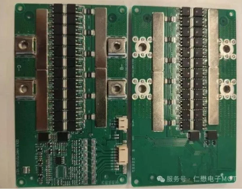
*Id = 80A: A single cell can handle considerable current, multiple cells connected in parallel easily meet continuous discharge demands of 120A or even higher (as shown in the board model in the image ).
*Extremely Low Rds(on) Typical Value: At Vgs = 10V, its on-resistance is only approximately 1.8mΩ. This means it is with very low power consumption and heat generation in the on-state, so as to extraordinarily improve system efficiency and thermal stability.
* Excellent Packaging: It typically uses TO-252 (DPAK) package to provide excellent heat dissipation while minimizing PCB footprint, and make it ideal for such space-constrained applications like BMS.
*In the BOM list, its role is clear and crucial: as an electronic switch, it executes commands from the MCU, safely connecting or disconnecting the main circuit between the battery and the load.
BMS Application Scenarios: Why This One?
Observing the BMS board in the diagram, the power path is clear: current flows in from the battery connector and passes through the sampling resistor, then through a row of paralleled MOSFETs (usually including two sets: charging control and discharging control), and finally flows to the output terminal.
1,To handle steady-state current: for the nominal 120A continuous current, connecting 3-4 pieces of MOT80N03D Mosfet in parallel, it easily controls the actual operating current and temperature rise of each device within a comfortable range. Its low Rds(on) characteristic directly translates into lower conduction losses and higher overall efficiency.
2, To handle transient shocks: Motor starting and load plugging/unplugging can generate pulse currents several times then the rated value. The MOT80N03D's large pulse current withstand capability ensures that it will not be damaged by over-current under these transients,and gives the protection circuit time to respond.
3, Simplified driver design: Its moderate gate charge allows common BMS-specific AFE chips or driver ICs to directly and efficiently drive multiple paralleled MOSFETs without the need for complex cascaded driver circuits, and simplify BOM and PCB layout.
From BOM to PCB: Reliability in Detailed Design
The circuit board layout in the image is a testament to good design and explains how components like MOT80N03D can be effectively utilized.
•Symmetrical parallel layout: We can see that the MOSFETs are neatly arranged. On the bottom layer of the PCB, their drain (D) and source (S) terminals are typically connected by large copper foils. This design ensures current sharing among multiple MOSFETs,so as to prevent premature failure of a single device due to overwork caused by asymmetrical layout. This is the key to maximize the capabilities of paralleled devices and achieve the nominal value of 120A.
•Thermal Design and Thermal Coupling: The DPAK package's metal plate is directly soldered to a large copper area on the PCB. This copper area serves as the primary heat sink. The heat is conducted to the back or other layers via the thermal vibrator to effectively control the junction temperature during operation. The BOM may also consider to apply thermal paste or install a heat sink in this area to handle more demanding operating conditions.
•Synergy of protection circuits: The BOM list will inevitably include precision sampling resistors and fuses near the MOT80N03D Mosfet. The sampling resistor is used to detect current in real time, working with the AFE/MCU to achieve over-current protection. The fuse serves as the last line of irreversible physical protection. The MOSFET, sampling resistor, and protection IC form a closed-loop protection network in the BOM and circuit.
Selection Considerations and BOM Costs
When creating a BOM, engineers will consider the following trade-offs when selecting devices like the MOT80N03D:
1. Voltage and current margin: 30V withstand voltage is sufficient for 7-series applications, but a higher withstand voltage model should be selected for more series. Current capacity needs to be calculated based on peak current and the number of parallel connections, with a margin of at least 30%.
2.Conduction Loss and Thermal Budget: Calculating the total conduction loss under full load, P_loss = I²Rds(on), and ensuring that the MOSFET junction temperature does not exceed a safe value (typically 125°C) at the expected maximum ambient temperature,these determine whether additional heat dissipation measures are needed or not.
3.System cost optimization: Although the cost of a single MOT80N03D Mosfet is very low, but in mass production of BMS, the large quantity makes its proportion of the total cost significant. Its high reliability and low failure rate can avoid the huge costs of after-sales maintenance. From a life-cycle perspective, choosing quality components with guaranteed is actually the most economical approach.
4.Supply chain security: As a domestic power semiconductor brand, Inmark has a stable supply of general-purpose models such as MOT80N03D, which helps ensure the long-term availability and price stability, which is crucial for mass production.
Conclusion: Small components, Great responsibility !
The reliability of a BMS is hidden in its BOM list and PCB layout details. Power MOSFETs suach as Inmark’s MOT80N03D, while not expensive, but are core execution units in the current path. Its stability and reliability directly determine whether the battery pack can safely "brake" under each abnormal condition.
For engineers, understanding the Bill of Materials (BOM) is not just about recognizing component models, but also about comprehending the design intent, safety boundaries, and cost considerations behind each component. Choosing components like the MOT80N03D, which have been proven in the market for a long time, balanced parameters, and reliably supplying, is to find the best balance between performance, cost, and risk, and is also a solid foundation for building a durable and safe BMS product.

 Headquarter: 19th Floor, SCTC Mansion, Guiyuan Rd, Luohu, Shenzhen, Guangdong
 Contact Phone:+86-755-82527851